Control an LCD module over I2C (TWI) with an avr
Published: 2023-Mar-19
Introduction
This article shows how to connect an atmega 2560-based board to an LCD module over I2C (Inter-Integrated Circuit). No I2C/LCD library will be used, the goal being to further the understanding of a beginner. The TWI (Two-Wire Serial Interface) used in the Atmel (now Microchip) documentation is basically the same as I2C. Those two terms will be used interchangeably here. The I2C is interesting here because it allows us to perform the desired task using only 2 pins of the microcontroller (MCU) instead of 8. The downside is that we need a new I/O expander board to bridge the gap between the 2 pins of the MCU and the 8 pins of the LCD module and we'll have a slightly longer code. The full source code is available on github. The main steps are: configure the TWI module, initialize the LCD and write a few functions to display some text or graphics or both.
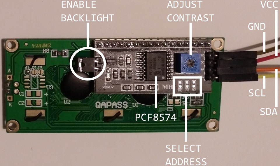
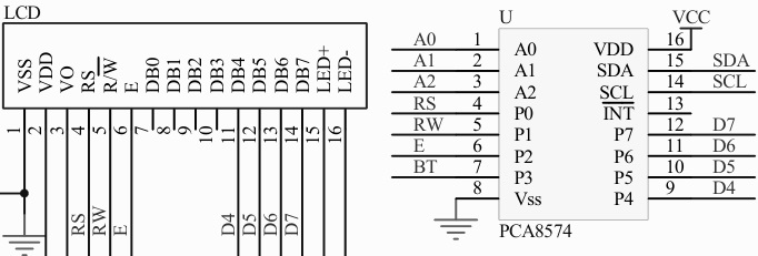
The left picture above shows the 8-bit I/O expander board soldered onto the LCD. The Jumper BL allows the backlight to work. The final control is achieved through software (BT_DATA).
Any atmega 2560-based board will work (as long as you can obtain the datasheet), because all the code will use the default atmel libraries. I'm using an Arduino mega 2560. Most Arduino clones probably have the same pinout [2] as the parent Arduino, but double check just to make sure and adjust the pins accordingly. Because the expander board already includes pull-up resistors on the SDA and SCL (clock) lines, we will neither be using additional resistors nor activating internal pull-ups on the MCU board. The circuit is powered through the USB port.
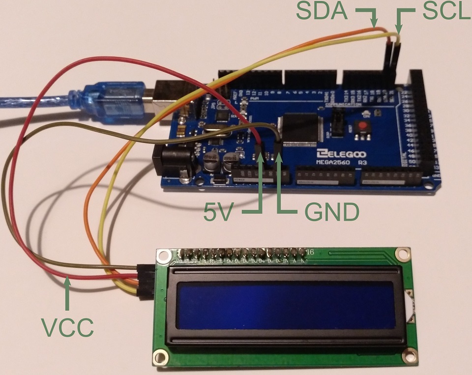
I2C configuration
The expander directs the incoming data frame from SDA to the pins {P0...P7}. In our case the pins {P0...P7} are connected to RS, RW, E, BT and {D4...D7} respectively. This will be important when formatting the data to be sent through the data bus.
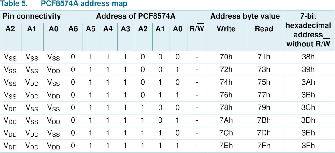
To communicate with the expander, we first send its address over the I2C bus, followed by a bit indicating whether we want to read from the bus or write. We then send a series of commands or display data or both. Once the final piece of data for the session has been transmitted, we release the communication bus. All these operations will be performed with a bus frequency of 100 kHz.
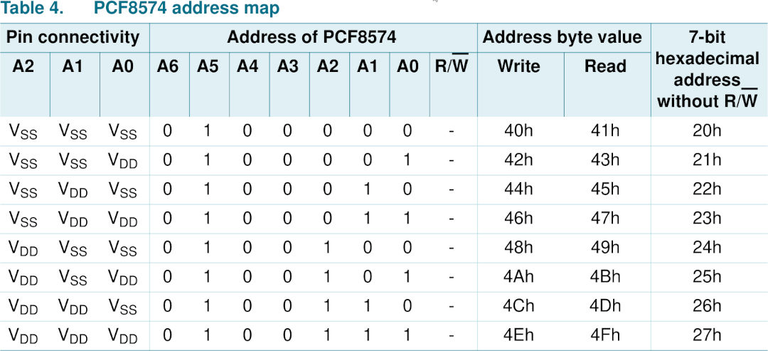
The address of the expander depends on the particular chip that's on the board (PCF8574 or PCF8574A) and the position of the jumpers on the back. The schematic shows the presence of pull-ups resistors on the pins A0-A2. So the address is 0b01001110 = 0x27. Any connected jumper would have changed the corresponding bit to 1.
The clock frequency is set by writing to the TWBR. The following formula shows how to calculate the right value for the desired SCL frequency. By default, TWPS0=TWPS1=0 and the CPU frequency is at 16MHz. So the resulting TWBR value is 72.

We will not be reading any data from the LCD module, so we can append the write bit (=0) to the address when initializing the device. The resulting writing address is 0x4E.
The error handling consists of retrying several times, if necessary, before moving on. There are very few things that can go wrong in a simple project like this, so we won't go overboard. Warning: Do not use this code, as is, in production 😅
Once the I2C has been initialized, sending bytes is pretty straightforward: load the data into the TWI Data Register (TWDR), set the correct bits in the TWI Control Register (TWCR), clear the TWINT bit (i.e. write 1) to execute the operation defined in TWCR, wait for the TWINT bit to be set by the hardware and repeat. The TWSR provides status information that could be useful to check if everything is behaving as expected. The bits of interest to us in TWCR are TWINT, TWEN, TWSTA and TWSTO.
- TWEN (TWI Enable):
- This is set to ensure the TWI module remains enabled.
- TWSTA (TWI Start):
- Writing this bit to 1 makes the TWI try to take control of the serial bus. If successful, the start condition is sent by the hardware module.
- TWSTO (TWI Stop):
- Generate the stop condition and release control of the bus.
- TWINT (TWI Interrupt):
- This bit has to be cleared (written to 1) in software (i.e. by our code) to start the execution of the operation defined by the other bits of TWCR. The I2C hardware (the I2C part of the avr) sets this bit to 1 once the operation is completed. This bit is not set after sending the stop condition, so we can skip checking it when stopping the transmission.
LCD Configuration
All the information needed to use the LCD module can be found in its datasheet. The Screenshots below reference the page number from this datasheet. Two important parts to understand are the initialization by instruction and the timing diagram.
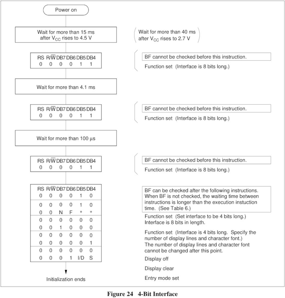
The module is in 8-bit mode by default. But given that the expander doesn't connect the data pins {D0...D3}, we'll switch to 4-bit mode. In this mode, 1 byte is sent by starting with the high-order half-byte (nibble) before sending the low-order nibble in a second operation. This is achieved in code by using masking and shifting. We choose to wait a little more than the minimum delay between operations.
lcd_init() performs the operations illustrated in the figure above.
send_over_twi() is responsible for initiating and completing bus transmissions.
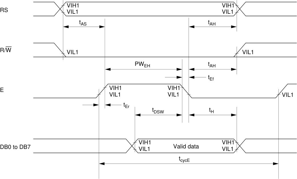
Here's how we'll implement the diagram [3]:
- Load the data bus, along with the signals BT, RW and RS.
- Pull the Enable line high and keep it that way for around 1us (> tEr). We then wait 50us after the line is down to give the controller enough time to execute the command.
RS is used to select which register of the LCD controller will receive the data. RS=0 when sending an instruction to the controller and RS=1 when sending (display) data. BT is constantly held high to keep the LCD backlight on.
lcd_enable() is responsible for handling the EN-signal. It is called every time the data bus ({D0...D7}) is loaded and only toggles the EN-bit in accordance with the timing diagram.
One example command we'll use is FUNCTION_SET_4B_2L, which will instruct the LCD to switch into 4-bit mode and display 2 lines. When 2 lines are requested, the display cannot fit 2 lines of 5x10 dot character font, so the only font available in this configuration is 5x8 dot.
Pulling everything together
All the work has been done in i2c.c and lcd.c and comes together in main.c. After some basic module initializations, lcd_print() writes the desired text to the display.
#include "i2c.h"
#include "lcd.h"

int main (void) {

	i2c_init();
	lcd_init();

	lcd_print("HELLO, WORLD!");

	while (1) {
		// This can be empty
	}

	return 0;
}
The data currently being displayed (a 32 character window) and the data to be displayed (the remaining 48) are copied into the Display Data Ram (DDRAM). When configured in 2 lines mode, the automatic line wrap will not occur at the 17th, but rather at the 41st character mark. It also automatically wraps around to the first position after the 80th character. lcd_print() can easily be extended to move the cursor as it's about to enter the 16-40 range.
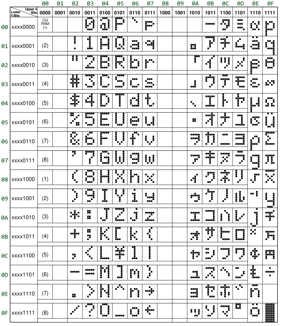
The code sent to the controller, to display a character is obtained by combining the nibbles read from the column and row of the desired character from the picture above. According to this, the code for the letter s is 0x73 while 0x37 corresponds to the digit 7.
Calling lcd_print() with special arguments, such as "ßüÜöÖäÄ", doesn't display the expected characters. The reason is because those special characters in the argument are each encoded in two bytes and the controller will output two (probably different) characters. The encoding is UTF-8, but the controller will decode it byte by byte using the character set table of the controller. The first byte maps to the Japanese character テ and the second one is a space character. The same process applied to the remaining bytes leads to the bottom part of the picture below.
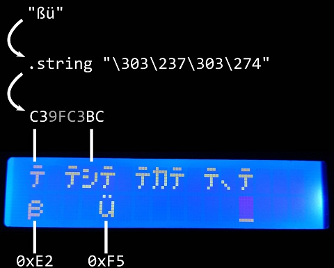
One easy way of actually displaying those characters (assuming no Kana are desired), is in checking the next byte every time 0xC3 is detected before sending the appropriate character code.
Custom Characters
Custom characters can be displayed by creating the corresponding patterns at the addresses that map to the first column of the character set table. There's enough space for 8 different patterns with a 5x8 dot font and 4 with a 5x10 dot font at a time. We'll only work on the 5x8 grid. The process is the same for the 5x10 grid. The picture below shows all the elements necessary to create 2 patterns.
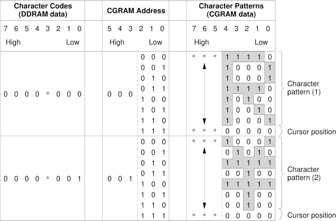
The stars (*) used in the table indicate, the bit can either be 0 or 1, the result is the same. One consequence is that multiple numbers can represent the same code. For instance, the last cell in the first column equals 0b00000001 = 0x01 = 0b00010001 = 0x11.
The pattern has to be designed on the grid shown in the rightmost column (CGRAM data). A black dot is represented by a 1, and a space by a 0. So that first row of the R pattern can be represented as 0b00011110 = 0x1E. To save that line, we need to write that value at the address shown directly to left, in the middle column (CGRAM Address). This process is repeated for all the lines of the pattern. Once done, the character code in the leftmost column will output the saved pattern.
Writing to a specific CGRAM address begins by sending the address byte to the controller as a command. The data corresponding to the pattern is then sent byte-wise to the controller. The address byte is of the form 0b01AAAAAA. Any one of the write operations to the CGRAM increments the address counter. So we just need to send the address of the first line. The starting address is calculated every time a pattern is saved. The address of the first pattern is 0b01000000 = 0x40, and increases by 8 for every subsequent pattern.
Because the address counter is automatically incremented each time we write into the CGRAM, the display cursor may need to be repositioned. The last step is to send the character code corresponding to the pattern we want to appear on screen to the controller. The on-screen characters are automatically updated if the CGRAM is edited.
One Last Picture
I'd like to think the code is pretty readable, so I haven't included snippets here. Let me know if you think otherwise. Only the basic configurations have been made here, but the code could easily be extended.

I hope you enjoyed this article. Thanks for reading.
Notes
- ↩ The schematic was confirmed using the continuity function of a multimeter. My board isn't from dfrobot, but this schematic seems to be standard.
- ↩ The pinout is useful to easily identify how the pins of the atmega are exposed on the board.
- ↩ Those delays are not strictly necessary in this code, because of the overhead of the I2C transmission. At 100 kHz, it takes around 80us to transmit 1 Byte through the bus.
References
- 8-bit I/O expander module - Schematic and PCF8574 datasheet
- Arduino Mega 2560 Rev3 datasheet (In the resources section)
- ATmega 2560 - Datasheet - 24. 2-wire Serial Interface
- LCD Controller - HD44780U datasheet
- UTF-8
- Source code on GitHub